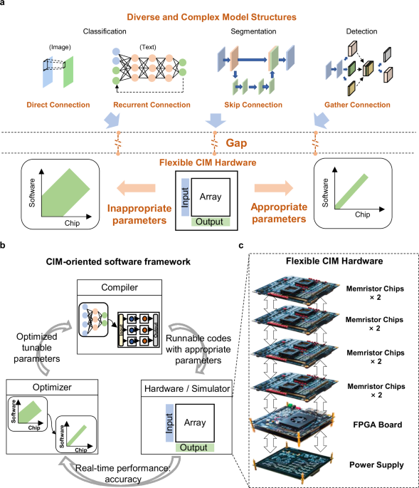
Full-stack CIM system for diverse models
We develop a flexible and computationally efficient memristor-based CIM system, as shown in Fig. 1c. The hardware features flexible memristor chips and an extendable system design. The fabricated memristor chips contain functional circuit modules for flexibly accomplishing on-chip MAC with signed inputs and weights. The system adopts pluggable printed circuit boards (PCBs) to load memristor chips. In this way, the system can improve the memristor capacity by adding additional PCB modules without turning off the power (see Supplementary Note 1). In addition, the system contains one power supply module and one field-programmable gate array (FPGA, Xilinx, ZU3EG) with a hardcore CPU (ARM, Cortex™-A53) as the global controller, as shown in Fig. 2a. The FPGA with the hardcore CPU can flexibly control different data flows from one memristor chip to another. All AI models operations can be accomplished on the hardware system without using external assistance.

a Schematic of the system with eight memristor chips, one FPGA board as the global controller and one power supply module. Each memristor chip contains the functional modules such as an input buffer, a memristor array and its input decoder, an output buffer, an ADC, and an on-chip controller. Die microphotograph of the memristor chip with 144k cells. b The CIM IR with three types of parameters and two types of computing units for optimizing parameters and generating hardware runnable codes. c The schematic of six different AI models and the automatic deployment flow.
A microphotograph of the memristor-based CIM chip is shown in Fig. 2a. The chip contains a memristor array, signed input circuit (SIC), analogue-to-digital converter (ADC), on-chip buffer, on-chip controller, etc. Each memristor array contains 1152 × 128 1-transistor-1-memristor (1T1R) cells. Two 1T1R cells are grouped into one 2-transistor-2-memristor (2T2R) cell to represent one signed 4-bit weight value. The memristor cell adopts a TiN/TaOx/HfO2/TiN material stack. The cells exhibit excellent programming precision and retention time for both 3-bit single cell and 4-bit grouped cells (see Supplementary Note 2). The materials and fabrication process (see Methods) are compatible with the conventional complementary metal–oxide semiconductor (CMOS) processes. In addition, compared to a conventional binary input circuit, which only supports 0 and 1 as input, the designed SIC uses the same amount of voltage source to support signed input data (−1,0,1), increasing the hardware flexibility with almost no extra overhead. And the high-speed and low-power ADC, which uses 15 dynamic comparators to work simultaneously, improves the system’s throughput and reduces power consumption (see Supplementary Note 3 and Supplementary Note 4).
The complexity of AI models not only demands greater flexibility from hardware but also imposes higher requirements on software. Because the model deployment of analog computing systems introduces not only the labor burden challenges but also those of computing accuracy requirements. In this work, we introduce CIM-oriented software, as shown in Fig. 2b, which features a unified CIM-oriented intermediate representation (IR) (see Methods ‘CIM IR’ section). Base on the CIM IR, we further implement an end-to-end compiler, which support multiple AI model structures and hardware features (see Supplementary Note 5 and 6). Compared to prior CIM-oriented software framework studies24,25,26,27, which only consider the basic functional support that detects the CIM-friendly operations and deploys them on the CIM hardware, the proposed CIM IR further consider the hardware-related parameters representation. These parameters are tunable and exposed by the hardware, which aims at keeping the flexibility of the whole system and obtaining better performance. For example, in previous work16, to adapt to the diverse output dynamic range of different models, the chip operating conditions can be manually tuned according to the input data and model weight. Hence, to facilitate a more convenient and uniform representation of hardware-related and algorithm-related parameters, we categorize all parameters into three distinct types: algorithm parameters, mapping parameters and calculation parameters. Algorithm parameters refer to the models’ attributes, such as the operation’s type, and the stride, kernel size, and padding in convolution layer. Mapping parameters refer to the computation physical address in hardware and layer parameters in AI models. These parameters are determined by the compiler frontend with the mapping method (see Supplementary Note 5). Calculation parameters refer to hardware tunable parameters such as ADC integration time (IT), weight copy number (WCN), and input expansion mode (IEM), which are owned in our hardware. These different types of parameters are denoted as ‘Attribute,’ ‘Mapping,’ and ‘Calculation’ in Fig. 2b, providing a unified and comprehensive representation. There are two key advantages to model deployment using this unified CIM IR. Firstly, the unified representation bridges the gap of automatically converting high-level operations into low-level hardware implementations—a process that was previously handled manually in prior works12,16. Secondly, the unified representation enables automatic optimization with software, which substantially enhances the efficiency of parameter tuning. In addition, to easily deploy the AI models, we divide all AI model operations into two types: CIM-friendly operations and other operations. The CIM-friendly operations refer to convolution, MVM, transpose convolution, etc., which can be accelerated using memristor arrays. Other operations refer to pooling, linear rectification function, etc., which are computed on the FPGA in our system. In the IR of our software framework, we use the ‘Virtual’ to represent non-memristor computing units and place all of the CIM-unfriendly operations on it. For CIM-friendly operations, the compiler generates runnable codes that are executed on memristor arrays. For the other operations, the compiler generates codes, which are executed on the FPGA in our system. In the future, in a well-designed SoC chip, other operations can be computed using specific digital modules or an on-chip general processor module. The detailed deployment process can also be found in Supplementary Note 5.
Utilizing flexible hardware and general software, we have successfully implemented six different AI models with an automated deployment approach on a memristor-based computing system. The six AI models include a two-layer MLP, a three-layer CNN, and a ResNet-32 for image classification, a single-layer LSTM network for text classification, a U-Net for image segmentation task, and a reduced RetinaFace-Net for object detection (Fig. 2c). The chosen models are widely used in various typical AI applications, and contain the most common AI models operations. In addition, these models also include the basic model topology structures such as direct connections in MLP, skip connections in U-Net and ResNet-32, recurrent connections in the LSTM network, and gather connections in reduced RetinaFace-Net. The detailed neural network model parameters and performance are presented in the Supplementary Table S1. The processes of execution and mapping of above models can be found in Supplementary Note 7 and Supplementary Fig. S8. The model placement methods for CIM systems are also studied in previous work28, which can also be integrated in our software framework. These demonstrations illustrate that the developed CIM system, equipped with the proposed software framework, can manage a wide range of AI applications. This capability eliminates the need for manual efforts, thus enhancing the practicality of the CIM system.
Beyond its automatic deployment capability, our proposed software framework further incorporates three optimization methods to automatically mitigate the analog computing noise resulting from the analog system nonidealities16, thereby enhancing the on-chip accuracy. These three optimization methods are applicable to the two main stages of maintaining on-chip accuracy: the training stage and the deployment stage respectively.
Post-deployment training
For the training stage, we introduce the post-deployment training (PDT) method (Fig. 3a), which aims at automatically improving the robustness of model weights against the system nonidealities during training phase. The PDT method is proposed based on two observations. On the one hand, we find that the conventional offline training methods, such as hardware-aware training (HAT)29, relied on the precise computing models of the hardware inference process. And these precise models are not intuitive and easy-understanding for the algorithm designers who are not familiar with the hardware characteristics. Hence, current model training still relied on the experts who are familiar with both hardware and algorithm, which significantly limit the algorithm development.

a The schematic of software work flow of post-deployment training. b Comparison of chip simulation accuracy between conventional training and post-deployment training. The error bar indicates the standard deviation derived from 10 repeated tests. c The software work flow of single-stage automatic tuning. d Comparison between pure software results and the fully on-chip MAC results without automatic parameter tuning. e Comparison between pure software results and the fully on-chip MAC results with automatic parameter tuning.
On the other hand, we find that the conventional training process overlooks the errors caused by two common operations in the CIM computing process. This oversight means that the conventional training process does not fully account for the hardware inference flow. First, the digital-to-analog convertor (DAC) of CIM hardware is often with low-precision, so the input data often needs to be split according to the bit width of the DAC (See Supplementary Fig. S12a). After splitting, the output result corresponding to each batch of DAC input data will lead to a quantization error for the final accumulated result. However, conventional HAT flow often quantizes only once after the input and weight multiplication and accumulation for the sake of model training convenience. This approach neglects the multiple quantization errors caused by bit-slicing. Second, when the algorithms are designed with large-size weights, the compiler will split these weights into pieces to adopt to the memristor array size (see Supplementary Fig. S12b). The output results from different pieces are also subject to ADC quantization error before accumulation. This further increases the discrepancies between the conventional training flow and the hardware computing flow. These computing processes with CIM characteristics have also been reported in other studies29,30.
Based on the above two observations, we propose the PDT method. This method not only recovers inference accuracy by training the model with an automatically generated hardware-consistent inference flow but also decouples algorithm design from hardware characteristics. Specifically, we adopt two critical designs to achieve this. Firstly, we customize the bit-level gradient backpropagation process in the training flow to keep the computation process consistent with the hardware’s bit-slice computation process. Secondly, since we cannot restrict the weight size of the algorithm to always meet the requirements of the array size, we use a ‘deploy-first-train-later’ approach for model training. That is, we use our software tools to deploy the model on the hardware virtually, which can get the CIM-IR with weight mapping information. And then, with support of the proposed software framework, we can generate new trainable neural network codes, such as Pytorch31 codes, according to CIM-IR and customized trainable module. Thereby, we can train the newly generated network codes to perceive the error problem caused by bit slicing and weight splitting. Notably, the entire training process is facilitated by our automated software framework, which markedly enhances training efficiency. And the customized trainable module can be provided by the chip vendor, which is invisible to the algorithm designer. This approach allows algorithm designers to remain unaware of the hardware characteristics, thereby alleviating the training burden on algorithm designers. The detailed implementation of PDT can be found in Methods section ‘Post-deployment training’.
To verify the effectiveness of the above methods, we implement both the conventional training and the post-deployment training methods for ResNet-32 model in Pytorch framework. To keep the training process consistent, both training processes use the same training parameters, i.e., learning rate, batch size, number of training epochs, input and weight quantization precision, weight noise amplitude. The detailed training process is shown in Supplementary Fig. S13a. The results reveal a very similar trend in loss reduction between the conventional training method and the PDT method, which indicates that our proposed method does not introduce additional training complexity. After training, two sets of different network weights are obtained. We use these two sets of weights to perform inference on a chip simulator, which contains all non-idealities of the memristor chip, as shown in Fig. 3b. The experimental results show that the PDT method can improve the inference accuracy by 4.76% compared to the conventional training method, while preserving friendliness to algorithm designer. Furthermore, we also evaluate this method using a large-scale network such as ResNet-50 for CIFAR-10032 classification. The model structure is shown in Supplementary Fig. S22, which contains 23.65 M weight parameters. The training process and test results are shown in Supplementary Fig. 13b, which show that the PDT method can get a 38.76% accuracy improvement. The results suggest that as network depth increases, the accuracy degradation becomes more pronounced. The primary reason for this is that with a greater number of layers, errors resulting from quantization and other non-idealities can accumulate substantially, resulting in an unacceptable on-chip accuracy. This result further confirms that the aforementioned mismatched errors have a significant impact on the model accuracy, especially for the deep models, and it also validates the effectiveness and necessity of the PDT method.
Single-stage automatic tuning
For the deployment stage, it is essential to identify the best hardware tunable parameters to reduce the analog computing error for well-trained models. The accuracy loss due to analog computing noise varies across different models. Larger networks with more on-chip layers tend to be more susceptible to analog computing noise16. Additionally, the effectiveness of using varying amounts of hardware parameters to reduce the analog computing error also varies. Generally, increasing the number of tunable hardware parameters is helpful in reducing the analog computing error, albeit at a higher optimization cost. Accordingly, different networks may necessitate distinct optimization strategies. To meet the diverse optimization demands during deployment stage, we have integrated a variety of optimization strategies into our software framework. Specifically, we introduce two strategies: Single-Stage Automatic Tuning (SSAT) and Progressive Two-Stage Search (PTSS). SSAT is specifically designed for automatically optimizing a single tunable parameter when deploying small-scale networks, such as MLP, 3-layer CNN, LSTM, reduced Retinaface-Net, and U-Net in this work. PTSS is adapted for automatically optimizing multiple tunable parameters when deploying medium-scale and large-scale networks, like ResNet-32 and ResNet-50 in this work. Through a combination of on-chip experiments and simulation experiments, we validate the effectiveness of two distinct optimization strategies across networks of varying scales.
For a single parameter identifying, previous work16 determined the reasonableness of hardware parameters by comparing the hardware output results with software results of a subset of training dataset. The software results can be obtained by using the CPU to inference the model with floating-point format. Inspired by this, we can automatically complete this process through the proposed software framework as shown in Fig. 3c. We introduce the SSAT method for the automatically identifying the hardware parameter, which use the proposed CIM IR to represent the tunable hardware parameters and use the chip-in-loop (CIL) search method to automatically determine the optimal hardware parameters. For our hardware, the IT of ADC is the most critical hardware parameter, which can directly determine the hardware output. The inappropriate IT of ADC can result in considerable errors in the output digital signal, which leads to a significant accuracy loss on model accuracy. We conducted experiments on the convolutional layers of a 3-layer CNN and the RetinaFace-Net, adjusting the IT and observing the impact of the output results on final accuracy, as shown in Supplementary Fig. S9. The results indicate that for both networks, inappropriate ITs indeed result in over 50% loss in model accuracy. Hence, the SSAT method mainly focus on the carefully adjusting the IT to minimize the impact of analog computing noise on model accuracy. The key idea of SSAT is to use a compiler-hardware-optimizer to iteratively find the best hardware tunable parameters for each AI model. By tuning the IT value of each on-chip layer, we can get different hardware outputs of the chosen training dataset. And then we can get the mean square error (MSE) between the hardware results and the software results. In this study, we employ a greedy algorithm to search for the optimal IT, iteratively traversing the IT values within the specified range until the MSE ceases to decrease. The detailed search process can be seen in Methods section ‘Chip-in-loop search in SSAT’. We utilize the MVM results, which represent distinct hardware outcomes with consistent input and weights but different ITs, to illustrate the efficacy of the SSAT method, as depicted in Fig. 3d and e. These results demonstrate that the SSAT method can decrease the MSE by over 30%. Through minimizing the MSE of each layer, we can get the optimal IT value of all on-chip layers automatically, thereby improving the on-chip accuracy of each model.
Progressive two-stage search
For multiple parameters identifying, we can transform the parameters identifying problem into an optimization problem focused on minimizing the model final output error between the software and the hardware. Specifically, without considering any non-ideal factors, we can obtain the software output, Outideal. By adjusting multiple hardware parameters, we can obtain the inference result, Outhardware, from the hardware. By continuously tuning these parameters to make Outhardware as close as possible to Outideal, the overall accuracy of the hardware will approach that of the software, thereby improving the on-chip inference accuracy. Therefore, we can convert the entire parameter search process into an optimization problem as expressed in Eq. (1), which aims to minimize the mean squared error (MSE) between Outideal and Outhardware. Considering the multiple parameters of our hardware, we incorporate two additional parameters, which are WCN, and IEM. Both of these parameters are instrumental in reducing analog computing noise. The effects of these parameters on the hardware outputs are detailed in Supplementary Note 7 and illustrated in Supplementary Fig. S9 respectively. Hence, Outhardware is determined by the model parameters (Model), IT, WCN, and IEM, as shown in Eq. (2). Additionally, in order to implement this model within a single system, we want all the copied layer weights to fit within a single system (8 chips). Hence, we need to add the capacity constraint as shown in Eq. (3), where N is the number of network layers deployed on the chip.
$${{\boldsymbol{Minimize}}}\; {{\boldsymbol{MSE}}}\left({{Out}}_{{ideal}},{{Out}}_{{hardware}}\right)$$
(1)
$${{Out}}_{{hardware}}=f\left({Model},{IT},{WCN},{IEM}\right)$$
(2)
$${\sum }_{i=0}^{N}({W}_{i}\times {{WCN}}_{i})\le 576\times 128\times 8$$
(3)
To solve the optimization problem, we introduce the progressive two-stage search (PTSS) method, which incorporates both simulator-in-loop (SIL) and chip-in-loop (CIL) search, as shown in Fig. 4a. Since the feasible solution space for the overall hardware parameters expands exponentially with the number of parameter types and the depth of the network, our objective in the SIL search stage is to identify the optimal hardware parameters within a vast search space. Specifically, we primarily use the genetic algorithm33 (GA) as the search algorithm and employ a chip simulator to approximate the hardware output. The GA is a very common and efficient method to solve multi-parameter optimization problems in a huge search space. The two critical processes of GA are representing ‘individual’ and getting ‘fitness’. In this work, we gather all hardware parameters corresponding to the on-chip layers together to represent the ‘individual’ in GA. And we use the MSE between the simulator results with tuned hardware parameters and the software results as the ‘fitness’ in GA. The optimization process of the GA is to minimize the MSE through tuning the hardware parameters of each on-chip layer. The detailed implementation of the SIL can be found in Methods section ‘Simulator-in-loop search in PTSS’. From this stage search, we can fix most of the optimized parameters among all hardware parameters, such as WCN and IEM in this work, as shown in Fig. 4b.

a The schematic of software work flow of progress two-stage search, involving simulator-in-loop search and chip-in-loop search. b The schematic diagram of the multiple parameters search process in this study. During the Simulator-in-loop (SIL) search, a majority of parameters can be fixed from a vast parameter space, including WCN and IEM in this study. However, due to discrepancies between the chip simulator and the actual hardware, some parameters must be refined during the Chip-in-loop (CIL) search, which is aimed at further reducing computing noise on the actual chip, such as IT in this work. c The trend of test set accuracy with the change in standard deviation of weight noise under three different optimization configurations: baseline, PTSS-1, and PTSS-2. d Comparison of the on-chip inference normalized mean square error for all layers in ResNet-32 using parameters searched with SIL search and parameters searched with both SIL search and CIL search.
To evaluate the effectiveness of SIL search, we conduct experiments on the ResNet-32 network using the SIL method, selecting 256 training samples as the model’s input to obtain the software output (see Supplementary Note 13). We use parameters optimized solely for IT as the baseline and observe improvements in model accuracy when multiple parameters are optimized. Our experiments focus on two scenarios: optimizing the IT and the WCN (PTSS-1), and simultaneously optimizing the IT, the WCN, and the IEM (PTSS-2). First, we observed the trend in MSE error changes during the GA’s iteration process in these two scenarios, as shown in Supplementary Fig. S14a. For PTSS-1, the GA is set with a population size of 100 and a maximum of 300 iterations. Since PTSS-2 involves more parameters, the population size is increased to 150, with a maximum of 500 iterations. As expected, the MSE decreases as the GA iterates. After optimization, we select the tuned hardware parameters corresponding to the lowest MSE during the optimization as the parameters for inference. We then perform inference using the chip simulator with CIFAR-10 test dataset. As depicted in Fig. 4c, the results demonstrate that an increased number of tunable parameters confer greater robustness against noise, consequently enhancing the accuracy of inference. Furthermore, we evaluate the SIL search using the large-scale network, ResNet-50. The optimization details are provided in the Methods section ‘Simulator-in-loop search in PTSS’. The experimental results are presented in Supplementary Fig. S14b, which also illustrate the effectiveness of SIL search on optimizing multiple parameters. Especially when the standard deviation of weight noise reaches 12% of the weight range, which is comparable to real chips noise, the inference accuracy can be improved by up to 3.39% relative to the baseline.
Through the SIL search, we have obtained hardware parameters that are more robustness against analog computing noise. Subsequently, we deploy the well-trained weights in the hardware and utilize the parameters derived from the SIL search to inference on chip. During on-chip measurement, we encounter two abnormal cases that could lead to accuracy loss, as depicted in Supplementary Fig. S15. In the first case, we find that the optimized parameters yield varying effects across different layers. As shown in the Supplementary Fig. S15a, for certain layers, optimized parameters do not necessarily reduce the MSE. We attribute this primarily to the simulator’s inability to fully simulate all the intricate details of system noise. To alleviate the burden of modeling, we add the same noise to the weights of each layer in the simulator. However, in reality, the write noise of weights and the read noise during on-chip calculation are not necessarily consistent across all layers due to the varied weight numbers, weight positions, and the programming accuracy. These factors result in some discrepancies between the parameters obtained from the simulator and the optimal parameters for the actual chip. In the second case, we discover that even with the same optimized parameters, the measured results on different systems can vary. As depicted in the example of Supplementary Fig. S15b, the same optimized parameters that reduced MSE compared to the ‘Baseline’ for System 1 actually increased the MSE for System 2. We think that this discrepancy arises from two main factors. First, there are differences between analog computing systems. Despite employing the same PCB design and power supply, variations in manufacturing can lead to differences in performance across systems. Second, there are variations between chips. Apart from the inherent fluctuations in analog computing, manufacturing deviations result in differences between chips. These variations, combined with the non-idealities of the analog computation array, collectively contribute to the distinct performances of the systems. However, these differences are not reflected in the simulator, and accurately modeling these non-idealities is highly complex and costly.
Hence, to further reduce the effect of differences between simulator and real systems, we introduce the second stage optimization method – CIL search, as shown in Fig. 4a. Due to the optimization conducted in the first stage of PTSS, we have already obtained reliable parameters that exhibit a relatively strong resistance to system noise within an extensive search space. Consequently, it is unnecessary to perform a comprehensive search for all parameters again. Building on the experience of CIL search in SSAT for single parameter, we have found that layer-by-layer adjustment on the target chips enhances adaptability. This adjustment involves tuning the parameters after weight deployment, aligning them more closely with the characteristics of the target system. This approach can mitigate the impact caused by the discrepancies between systems and chips. Therefore, in this stage, we also employ the CIL search method to further refine the parameters of each layer on chips after weight deployment. During this stage, we still primarily focus on adjusting the IT of each on-chip layers as shown in Fig. 4b. There are two reasons to choose IT as the on-chip search parameter. First, other parameters influence the choice of IT, and adjusting them would expand the search space, thereby increasing the on-chip search cost. Secondly, compared to other hardware parameters, IT has a more pronounced direct impact on chip results, making it a more efficient choice for enhancing on-chip accuracy. The detailed process of CIL search in PTSS can be found in Methods section ‘Chip-in-loop search in PTSS’.
Utilizing the CIL search method, we conduct experiments on chip. In these experiments, we set the search range to ±500 ns around the IT optimized in the first stage. For above-mentioned two abnormal cases, we obtain the on-chip results after CIL search, which are depicted in Supplementary Fig. S16. The experimental findings indicate that the on-chip search in the second stage achieves two significant improvements. Firstly, it further reduces the computing error of the parameters obtained from the simulator in actual on-chip measurements. Secondly, it overcomes the issue of parameter mismatch caused by discrepancies among different systems. This approach can maintain the analog computing noise of various systems at a relatively lower level. In addition to this, we also evaluate the impact of the CIL method on reducing the MSE for all on-chip layers of ResNet-32. The results are presented in Fig. 4d, where the vertical axis represents the normalized MSE, and the horizontal axis indicates the names of the on-chip layers of ResNet-32. The experimental results show that the CIL method can further reduce the MSE by 15.54% averagely compared to the SIL method. This enhancement in robustness against system noise and discrepancies underscores the effectiveness and necessity of the CIL optimization in PTSS.
On-chip inference demonstrations
Finally, we utilize the flexible CIM hardware and full-stack software framework to automatically implement on-chip inference for all models in Fig. 2c. The training process and used datasets of all demonstrated models can be found in Supplementary Note 12. Applying the SSAT optimization method, we optimize five small-scale models, including MLP, 3-layer CNN, LSTM, reduced Retinaface-Net, and U-Net. The automatic optimized IT of ADC for each model is detailed in Supplementary Table S2. We conduct a comparison among three experimental sets: software results with 4-bit weights (Ideal software (4-bit weights)), chip measurement with SSAT, and chip measurement without SSAT. The configuration in the case of chip measurement without SSAT set the IT of last on-chip layer to 100 ns for each model, aligning with the default value of the system in this study. The experimental outcomes in Fig. 5a reveal that, through the utilization of the automatically tunning method, the classification accuracy of the 3-layer CNN model reached 95.87%, which is only 1.08% lower than the 4-bit software results. The average accuracy across all demonstrated small-scale models is 1.93% lower than the 4-bit software results. Additionally, the optimized on-chip inference accuracy demonstrates improvements of 5.40%, 9.12%, 4.99%, 9.45%, and 7.87% for the MLP, CNN, LSTM, U-Net, and reduced RetinaFace-Net, respectively, in comparison to the chip measurement without SSAT.
Through the SSAT optimization method, we have been able to significantly improve the on-chip accuracy in multiple small-scale AI models and effectively improve the efficiency of model deployment. For larger neural network models with more layers on chip, the analog computing noise accumulates layer by layer. In such cases, the simple and efficient method of tuning the IT becomes insufficient, leading to a significant reduction in final accuracy. As shown in Fig. 5b, we deploy the ResNet-32 network with 33 convolutional layers and 1 fully connected layer on the memristor chips to recognize the CIFAR-1032 dataset, which comprises 10,000 test images. The model structure and mapping locations on chips are shown in Supplementary Fig. S11. Although we conduct PDT method during the model training phase and optimize the IT during deployment phase using the SSAT method, the on-chip inference accuracy is still 4.05% lower than the software simulation accuracy with 4-bit weight (decreasing from 87.4% to 83.35%), which is unacceptable.
To maintain the on-chip inference accuracy for deep models, we employ the proposed PTSS method to conduct on-chip measurement experiments with the ResNet-32 model within the developed memristor-based system. We perform on-chip inference experiments for three scenarios: optimization of IT using SSAT (Baseline), optimization of IT and WCN using PTSS (PTSS-1), and simultaneous optimization of IT, WCN, and IEM using PTSS (PTSS-2). The experimental results are illustrated in Fig. 5b. The results demonstrate that, with the increasing number of optimization parameters, the on-chip accuracy at each node has been significantly improved, highlighting the effectiveness of the proposed optimization strategies. In the case of parameter optimization involving only the increase in WCN, the on-chip measurement accuracy is improved by 1.91%. When both WCN and IEM are all involved, the accuracy is further enhanced by 1.41%, as shown in Fig. 5c.

a Comparison of the accuracy between software results with 4-bit weights, on-chip results with SSAT, and the on-chip results without SSAT of various AI models. b CIFAR−10 classification accuracy at different model layers. From left to right, each data point represents a block of model layers inferenced on chip. The layers on the x-axis are the ReLU layers in the model, which are renamed by our software tool. The accuracy at a layer is evaluated by using the on-chip results from that layer as inputs to the remaining layers that are simulated in software with non-idealities. Three curves compare the test-set inference accuracy between the optimizing integration time only (Baseline), optimizing the integration time and weight copy number (PTSS-1), and optimizing the integration time, weight copy number, and input expansion mode (PTSS-2). c Comparison of software results with 4-bit weights, simulated results with 4-bit weights including all non-idealities, and on-chip results with optimizations under three configurations: Baseline, PTSS-1, and PTSS-2. The error bar indicates the standard deviation derived from 10 repeated tests. d Comparison of on-chip inference results under different systems with optimizations of Baseline, PTSS-1, and PTSS-2.
Furthermore, we also note a significant reduction in the discrepancies of on-chip accuracy across different systems when employing the PTSS method. As depicted in Fig. 5d, using the same CIFAR-10 test dataset, we conduct experiments on two separate systems. The experimental results suggest that the PTSS method effectively improves the on-chip accuracy and mitigates the impact of system discrepancies on accuracy. Consequently, both systems exhibit considerable enhancements in accuracy as the number of optimization parameters increases, achieving up to 3.32% and 4.84% improvements on model accuracy for system 1 and system 2, respectively. Furthermore, despite system discrepancies, the PTSS method ensures minimal variation in on-chip inference accuracy across different systems, significantly reducing the accuracy discrepancy by up to 0.88% (from 1.2% to 0.32%). The experimental results illustrate that the PTSS method effectively reduces the effects of fluctuating model accuracy resulting from system discrepancies, thereby enhancing the consistency of AI models inferencing across different analog computing systems.